| HP38G 64k RAM How-To |
|---|
| Image |
Steps |
| - none - |
When opening a '38G a while back, I recognized that HP thought of a few options in the layout of its board: a) the board can handle a 32k RAM chip or a 128k chip at the same position (see also HP Journal 4/94 pp. 6) and b) the board is prepared to carry a 32pin DIL ROM chip. "Hell," I thought, "should be possible to have more than the 22k currently available." After a few days of moderate work I came up w/ a patched ROM image that is able handle 64k RAM instead of 32k (at the cost of the DEMO routines...) while beeing fully backwards compatible ! All userRPL ApLets ever written (eg. using HPs ADK) will run just fine ! Also all systemRPL ApLets not directly accessing RAM based variables at F0000+ run very well (see also Software Considerations below).
In short: to upgrade the '38G, you'll have to open it and replace the ROM and the RAM chips... If you aren't brave-hearted, well, enjoy the pictures ;-)
For the upgrade, you need some hardware:
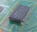
A chip to replace the build-in OTP ROM. This may be a 32pin DIL EPROM chip, eg. AMD 29C040-120, or alternatively a Flash-ROM chip, eg. AMD 29F040-12. For this kind of chips, I would recommend the Flash-ROM over the EPROM because it consumes less power, but unfortunately flash chips have JEDEC RAM pinout -- pin 1 and pin 31 need to be swapped...
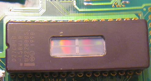
For an easier update you should use a 32pin SOP OTP ROM (if you can program them)-- eg. a NEC D27C4001GW-15 or a MX 27C4000MC-15 (both used in the '38G), and just replace the build-in OTP w/ it. In general, try to get a chip w/ the shortest access timing possible (even a 150ns will do it fine) -- the faster the chip, the less power it'll usually consume. Avoid the EPROM type I used, it's specified w/ 30mA while active...
If you decide to use a 32pin DIL chip, you may want to socket it (I wouldn't recommend that at all) -- I'd suggest to use single-pin sockets (like the one I used) -- they will leave enought space for inspecting the pads after the soldering job
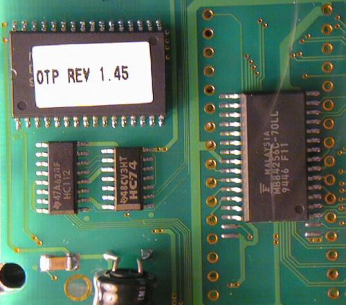
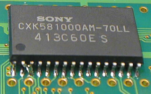
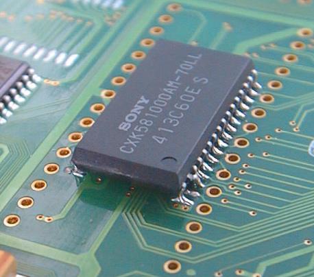
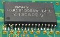
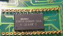
A chip to replace the build-in 28pin SOP RAM. Because there're no 64k RAM chips, we will use a 128k chip and restrict it to 64k. The new chip must be a 32pin SOP RAM conforming to the JEDEC pinout standard w/ an extra chip select line at pin 30 -- I used a Sony CXK 581000AM-70LL (they're in older '48GX units, unfortunately Sony discontinued them). I've read that Hitachi HM628128LFP-8 and one named KM 681000BLG-7L will work too, but I can't confirm that. The build-in 32k chip is a Fairchild MB 84256C-70LL, probably they offer a 128k version too
I used a socketed DIL ROM instead of an SOP OTP for an easier ROM update process after fixing bugs, the patch available should be bug free so you should use an SOP OTP to ease the upgrade. If you use a DIL type chip, I suggest not to socket it. However, I'll point out the differences in the following description.
After you got those chips, start over with creating the new ROM image to be programmed into the new ROM chip. First, grab this file: ROM upload for the '38G by JYA (3k) and follow the included instructions (README.TXT) to create an image of your current ROM on a PC. Now get this file: ROM patch for the 64k RAM upgrade (32k) and follow the included instructions to create the new ROM image. Program the new image into your new ROM chip and, if all went fine, get used to the idea of opening your '38G -- you may want to take a look at the DEMO at this point, last chance to view it... :-)
|
 |
Remove the battery compartment cover, the batteries and the sliding cover. To open the '38G it's neccessary to lift the keyboard overlay (those green plastic sticker where the keys shifted functions are printed at). Carfully heating the keyboard w/ a hair-dryer makes the glue a bit softer. Start w/ the edge below the [ON] or the [+] key and lift the overlay at least to the [ENTER] row. Between the [DEL] and the [ON] key-rows you'll see four little holes, between the [A..Z] and [SHIFT] key-rows two of them. Those are actually the heads of plastic rivets (a.k.a. heat-stakes), holding the unit together at the battery compartment. Use a 4mm drill operated by hand and drill their heads off, <1.5mm deep. The small picture shows one of the rivets on a '48G, they just look the same on your '38G. On the huge picture you can see them w/ heads off in the left/top half of the case. After the rivets heads are gone and the case is loose, reattach the overlay. You may later use a few very small screws to secure the case again (the rivets are hollow), but IMVHO that's not neccessary if you handle your '38G w/ some care.
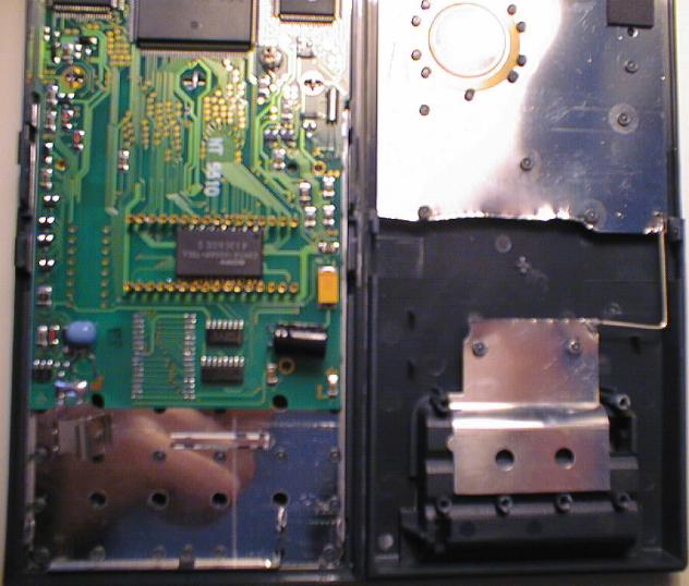
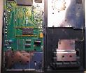
Carefully start to pull apart the case near the battery compartment, track the batteries "+" contact -- it may be neccessary to slightly bent in towards the "-" contact to unlink it from a small plastic hook that is part of the case. Apply some force w/ a fingernail in the groove between the case halfs near the LIB key-row, left and right, to unlink the hooks. Work towards the LCD w/ the fingernail along the lower edge (towards the bottom) of the big groove (where the cover slides in) to unlink two smaller hooks on each side. Carefully lift the bottom further unless the two big hooks around the serial connector release the bottom. You should end with the top (carrying the keys, LCD and board) and bottom (carrying the shield and piezo) halfes in your hands as seen on the huge picture.
You may now restart breathing ;-) -- put the '38G safely away, relax and examine what's in the machine to get used to it.
|
 |
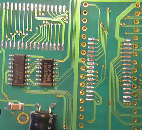
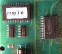
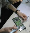
The pictures to the left show what to do next: you'll have to desolder the old ROM and RAM chips. Before heating the soldering iron, I suggest to do all things neccessary to avoid static discharge. This will keep the risk of damaging your '38G as low as possible.
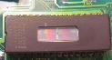
Don't wonder about the strange label on the ROM in the upper picture, the unit I's modifying is a very early prototype and thus was just useless (incompatible) before the modification (I've more than one '38G, BTW) -- your original ROM should be labled "ELSIE OTP REV 1.67". Machines made in Indonesia contain an SOP ROM, so the chips aren't labled anymore -- the ROM version is printed directly onto the chip ("VER 1.67"). |
 |
The next step is to solder in the new RAM chip. Before you start soldering, bend its pins a bit towards the plastic carrier (I used a small pliers -- grab the chip an apply some force), making it smaller to fit on its pads w/o causing shortcuts. Leave pin 2 out in this process ! Solder the chip and also here, leave pin 2 out (important !). Note: in case you decided to use a DIL ROM w/o a socket, try to solder the RAM as low as possible to the board -- you'll need every tenth of a mm to avoid cutting out the shield (see below).
After the chip is settled, carfully bent pin 2 towards pin 3 and solder pin 2 to pin 3 -- this will make the 128k chip acting as a 64k chip. Note that it's currently not possible to have 128k of RAM in the '38G w/o further major modifications in the ROM, so don't even think about leaving out the RAM crippling -- it won't work w/ this ROM patch !
It's very important that you carefully check your work (I'd suggest using a needle and a lens) -- make shure that the chip is aligned correctly, that there are no shortcuts between the pads and that all pins of the chip are definitely soldered to their pads ! |
 |
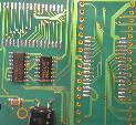
If you are going to use the SOP OTP instead of a DIL ROM (good choice !), solder it to its position now and continue here -- after you checked your work like you did w/ the RAM chip !
You may solder in the new ROM directly over the RAM chip (to prevent you from cutting out the shield later on -- note the allignment of the chip !) or solder in a socket. The pictures to the left show the socketed variant. Note that you need to solder the socket/chip from the component side of the board and that you eventually have to shorten the socket pins w/ an electronics cutter -- else they may contact the shield below the board and cause shortcuts !
If you use a DIL Flash-ROM, bent pins 1 and 31 upwards (~70°) before setting the chip. Use some thin wire to connect pin 31 to pin 32 and pin 1 to hole 31 on the board.
Again, it's very important that you carefully check your work here too ! If all looks well and you used a socket, carefully plug in the ROM -- note the allignment !
|
| - none - |
Now is the time to test the '38G basic operation. Apply some power to the unit (using a power-supply or an extern battery compartment w/ three AAA cells and two cables w/ crocos at both ends), watch out the polarity of the power connectors. Connect another cable to ground ("-") and slightly tip w/ its other end to the reset-pad on the board (a fat dot-shaped pad -- use the reset tongue in the back cover shield to locate it on the board). Turn over the unit and press [ON]. After ~3s it should come up w/ the HOME view. Issue an coldstart by pressing [ON]-[SK1]-[SK6] simultanousely, then releasing the keys. Press [OK] to get rid of the "Memory clear !" message, re-entering the HOME view.
Press [ON]-[SK4] to enter test mode (you should see three vertical lines on the LCD). Press [SK3], "IROM OK" should appear after a while. Now press [SK4], this should result in "IRAM OK" after ~2s. You may press [PLOT] to run an ESD check (press any key to cancel it). Press [ON]-[SK3] to leave test mode, then knock the '38G into COMA using [ON]-[,]. Remove power and continue w/ the next step.
If you experience any different behaivior from the test process described above, immediately remove power and check your work again ! Make shure there're no shortcuts and that all pins are safely soldered to their pads until you found the problem. Start over w/ the test. Repeat this procedure until you found all problems. If it still won't work, well your '38G might be dead, sorry :-(
Here's a list of RAM/ROM connections you can check w/ a DVM:
Name        RAM pins        DIL ROM pins    SOP ROM pins
----        --------        ------------    ------------
GND         1,16,24,30      16,24           16,24
VDD         32              1,32            1,32
D0          13              13              13
D1          14              14              14
D2          15              15              15
D3          17              17              17
D4          18              18              18
D5          19              19              19
D6          20              20              20
D7          21              21              21
A0          12              12              12
A1          11              11              11
A2          10              10              10
A3           9               9               9
A4           8               8               8
A5           7               7               7
A6           6               6               6
A7           5               5               5
A8          27              27              27
A9          26              26              26
A10         23              23              23
A11         25              25              25
A12          4               4               4
A13         28              28              28
A14          3              29              29
A15         31               3               3
A16          2               2               2
A17          -              30              30
A18          -              31              31
NCE         22              22              22    not connected !
NWE 29 - - |
 |
If you have soldered in an SOP OTP, skip the next two paragraphs and proceed w/ closing your '38G.
If you have soldered in a DIL ROM directly (w/o a socket), you need to cut of the head and the stake of the rivet holding the shield just above the DIL ROM using a good knife or electronic cutter -- you can see its position on the picture to the left, it's the cross in the middle of the area w/ the shield cut away. Skip the next paragraph and proceed w/ closing your '38G..
The piggy-pack you created may cause trouble when trying to close the unit, in this case use a metal-sissor to cut away the shield mounted in the back cover as shown in the picture to the left. Also remove the one stake holding the shield in this area. To keep the beeper and reset hole working, you should reconnect the bottom and top halves of the shield by soldering in a wire. Make shure the shield won't cause any shortcut to the ROM pins when the unit is assembled !
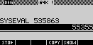
To close the '38G, start at the upper side (where the serial connector and the IR window are) by hooking the top and bottom halves of the case together. Press the them together until it unit looks like a '38G again -- watch out for the hooks to safely snap into their positions. You may attach some superglue to the edges of the bottom case to fix it, but IMHO that isn't neccessary (if you handle your '38G w/ some care). Mount the sliding cover, insert some batteries, close that battery compartment and press ON to verify the units operation. Key in SYSEVAL 535863[ENTER] while in the HOME view to get the amount of free memory, ~55355 bytes ! |
| Software considerations |
 |
On a 32k '38G the RAM is normaly configured to start at address #F0000, on the 64k '38G this is changed to #E0000 (#20000 nibbles --> 64k bytes). To keep the changes as small as possible, I disabled the ROM code in the address range #E0000 to #F0000, ie. the DEMO engine.
The modification affects the following supported entries:
=DemoFrames  EQU #E03A1    sRPL, points into the RAM now !
=DoDemo      EQU #821C5    sRPL, now does a NOP
=UnpackGrob  EQU #824BD    sRPL, now does a NOP
=~xxDEMO     EQU #038701   uRPL ROMPTR, now does a NOP
=uart_buffer EQU #F02B8    RAM addr, must be taken care of !
The patched ROM knows and handles the new start address, but any sRPL/assembler level program expecting the RAM at address #F0000 (eg. some games) or using DemoFrames (no ApLet known yet), UnpackGrob (no ApLet known yet) and/or uart_buffer (PLDL 100 ApLet, fixed version available) will fail to work and may even cause unpredictable problems, leading to memory losts in the worst case. So if you're loading a new game, back up your '38G before giving it control !
How to access RAM based variables formerly located at #F0000+ in a safe way in assembler:
D1=(5) =uart_buffer
could be replaced by
=IRAM@  EQU     #11F

        RSTK=C
        P=      4
        D1=(5)  =IRAM@
        C=DAT1  P
        D1=C
        P=      0
        C=RSTK
        D1=(4)  =uart_buffer
If you don't need to preserve C, remove the RSTK=C and C=RSTK instructions.
Upon return from =$jSAVPTR, D0 points into the updatable RAM section -- preserve its highest nibble w/in the CODE object and use D0=(4) =ram_addr to reload D0...
...TBC... |
| Credits |
- HP -- for the '48 and '38G, funny stuff to play w/ !
- Robyn Binder -- for picking up the draft version of this text and making a real document out of it !
- Jim Donnelly -- for his support on '38G related questions and for signing my copy of "An Introduction to HP48 System RPL and Assembly Language Programming" (ISBN 1-879828-06-5) -- thanks !-)
- Klaas Henschel -- co-founder of KLATHO GmbH & Co KG for his kindly support on hardware issues, for taking the pictures and the genius hint to just connect A16 to another A pin for limiting the RAMs address space to 64k
- Thomas Völker -- chairman of KLATHO GmbH & Co KG for organizing the chips
- Jean-Yves Avenard -- for his ROM upload ApLet, for the SAVPTR hint and for the one or other bit of information
- Paul Smith -- for his HP48G UPGRADE document somewhere lost in the WWW space... I captured the heat-stake detail picture and the part no. for the RAM chips from his description
|
| [To the top] |